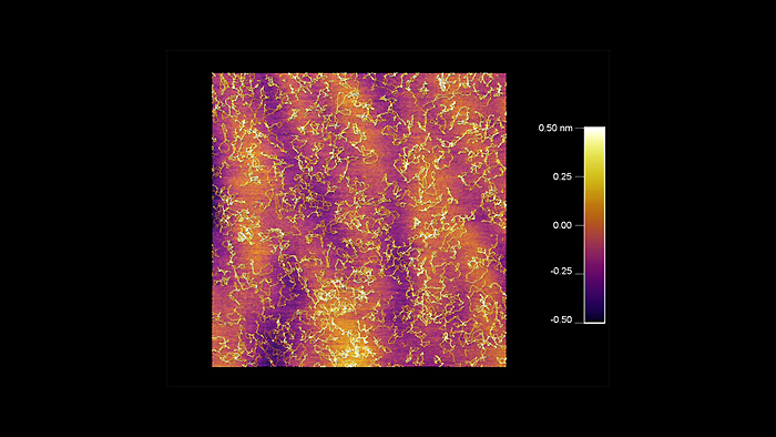
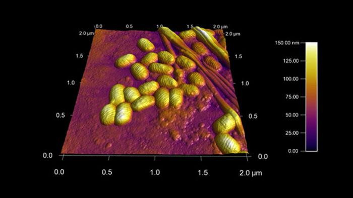
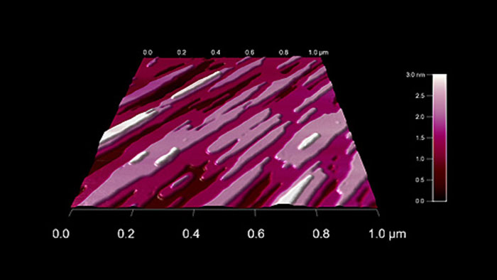
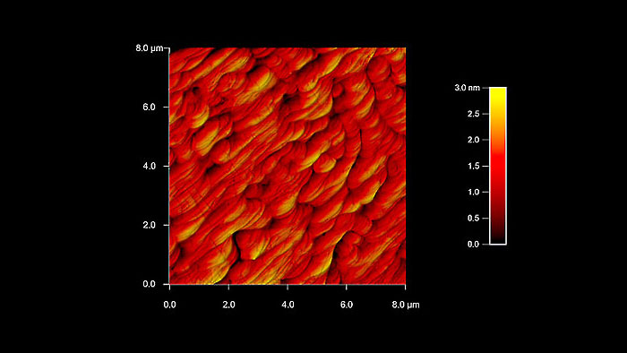
乾燥後のDNAの表面形状
Scanned with a BudgetSensors Tap300Al-G AFM probe on an Asylum Cypher AFM system, 5 micron scan size
Image courtesy of Scott MacLaren, University of Illinois at Urbana-Champaign, USA
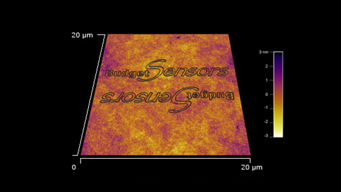
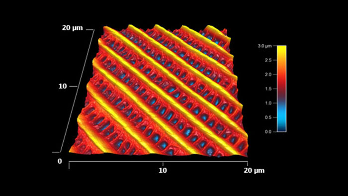
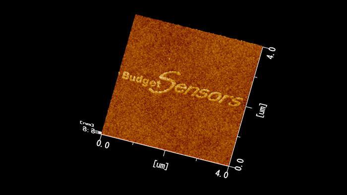
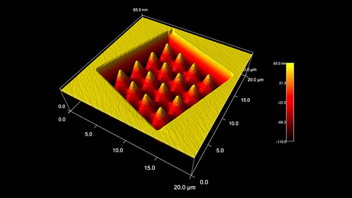
ポリカーボネートにスクラッチリソグラフィで描画したBudgetSensorsロゴ BudgetSensors Tap300Al-G使用AFMはAsylum MFP 3D
Scanned with a BudgetSensors Tap300Al-G 20umスキャン Asylum MFP 3D AFM システムで測定
Image courtesy of Scott MacLaren, University of Illinois at Urbana-Champaign, USA
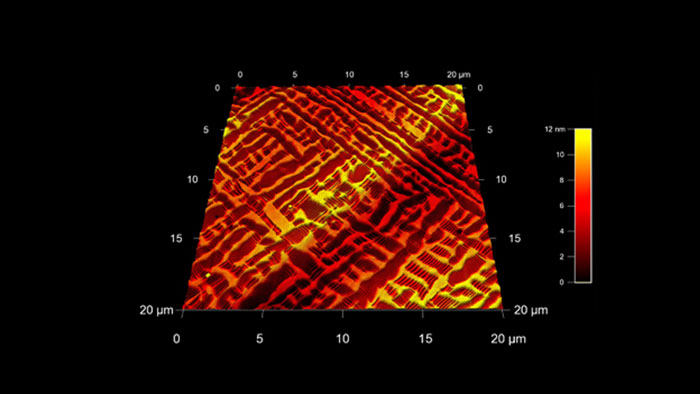
ランタンアルミネート(LAO)上のビスマス系イオンオキサイド薄膜 (BFO)
Scanned with a BudgetSensors Tap300Al-G Asylum Cypher AFM システムで測定 20umスキャン
Image courtesy of Scott MacLaren, University of Illinois at Urbana-Champaign, USA
Scanned with a BudgetSensors Tap300Al-G 4μmスキャン Tap300Al-Gで測定 Asylum Cypher AFM システム使用
Image courtesy of Scott MacLaren, University of Illinois at Urbana-Champaign, USA
ポックスウイルス
Scanned with a BudgetSensors Tap300Al-G Asylum MFP 3D AFMシステムで測定 2umスキャン
Image courtesy of Scott MacLaren, University of Illinois at Urbana-Champaign, USA
オレンジの皮の表面
Scanned with a BudgetSensors Tap300Al-G 10 umスキャン
Image courtesy of Scott MacLaren, University of Illinois at Urbana-Champaign, USA
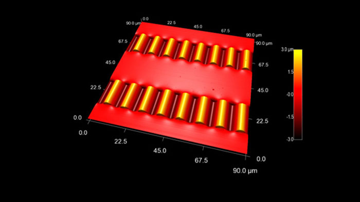
柔軟性のあるPDMS基板上に作られたシリコンナノリボン
Scanned with a BudgetSensors Tap300Al-G Asylum MFP-3D AFM システムで測定 90umスキャン
Image courtesy of Scott MacLaren, University of Illinois at Urbana-Champaign, USA
zipディスクのMFM測定
Scanned with a BudgetSensors Multi75M-G Asylum MFP-3D AFM システムで測定 75umスキャン
Image courtesy of Scott MacLaren, University of Illinois at Urbana-Champaign, USA
超電導量子フォトンディテクタ
Scanned with a BudgetSensors Tap300Al-G Asylum MFP-3D AFMシステムで測定 25umスキャン
Image courtesy of Scott MacLaren, University of Illinois at Urbana-Champaign, USA
マウスの筋線維
Scanned with a BudgetSensors Tap300Al-G Asylum MFP-3D AFM システムで測定 20 umスキャン
Image courtesy of Scott MacLaren, University of Illinois at Urbana-Champaign, USA
ポリマー表面の結晶構造
Scanned with a BudgetSensors Tap300Al-G Asylum MFP-3D AFMシステムで測定 3umスキャン
Image courtesy of Scott MacLaren, University of Illinois at Urbana-Champaign, USA
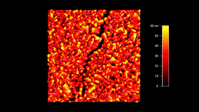
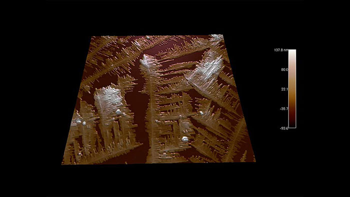
ナイトライド薄膜のクラック
Scanned with a BudgetSensors Tap300Al-G Asylum Cypher AFM システムで測定 2umスキャン
Image courtesy of Scott MacLaren, University of Illinois at Urbana-Champaign, USA
水でエッチングされた石膏の結晶構造
Scanned with a BudgetSensors Tap300Al-G Asylum Cypher AFM システムで測定 3umスキャン
Image courtesy of Scott MacLaren, University of Illinois at Urbana-Champaign, USA
クォーツ上のカーボンナノチューブ バンドル構造とクォーツの原子ステップが見える
Scanned with a BudgetSensors Tap300Al-G Asylum Cypher AFM システムで測定 3umスキャン
Image courtesy of Scott MacLaren, University of Illinois at Urbana-Champaign, USA
蛾の羽の表面形状 このナノ構造により、羽は疎水性をもち、かつ水に対し方向性を持つ。 水滴は常に体から羽の末端に向かって流れ、体をドライに保つようになっている。
Scanned with a BudgetSensors Tap300Al-G Asylum Research MFP-3D AFM システムで測定 20umスキャン
Image courtesy of Scott MacLaren, University of Illinois at Urbana-Champaign, USA
PDMS上のシングルウォールカーボンナノチューブ 水平面方向に圧縮するとナノチューブが波状に変形する
Scanned with a BudgetSensors Tap300Al-G 10 umスキャン
Image courtesy of Scott MacLaren, University of Illinois at Urbana-Champaign, USA
シリコン基板を陽極酸化した BudgetSensors ElectriTap300-G使用 JEOL JSPM-5200 AFM システムで測定
Scanned with a BudgetSensors Tap300E-G 4 umスキャン
Image courtesy of Takashi Sueyoshi JEOL Ltd, Japan
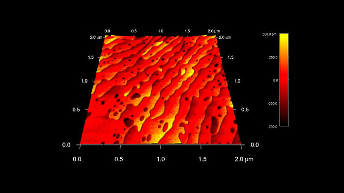
畝状構造のあるPDMS上のシングルレイヤーグラフェン
Scanned with a BudgetSensors AIOAl AFM probe, soft tapping mode cantilever (C), 10 micron scan size
Image courtesy of Scott MacLaren, University of Illinois at Urbana-Champaign, USA
SEBS ブロックコポリマーの位相イメージ 表面形状を3Dで表示し、位相イメージをカラーデータとして重ね合わせて表示した
Scanned with a BudgetSensors Tap300Al-G AFMプローブ, 4 umスキャン
Image courtesy of Scott MacLaren, University of Illinois at Urbana-Champaign, USA
ゼインタンパク質とコレステロール
Scanned with a BudgetSensors Tap300Al-G AFM probe, 15 micron scan size
Image courtesy of Scott MacLaren, University of Illinois at Urbana-Champaign, USA
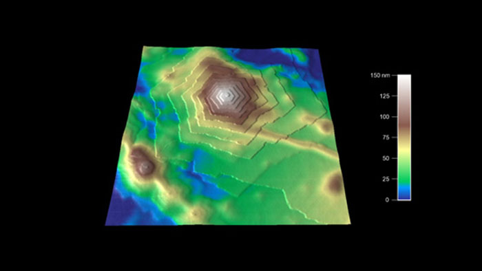
パラジウムの原子ステップ
Scanned with a BudgetSensors Tap300Al-G AFM プローブ 8umスキャン
Image courtesy of Scott MacLaren, University of Illinois at Urbana-Champaign, USA
湾曲した人間の毛髪
Scanned with a BudgetSensors Tap300Al-G AFM probe, 35 micron scan tsize
Image courtesy of Scott MacLaren, University of Illinois at Urbana-Champaign, USA
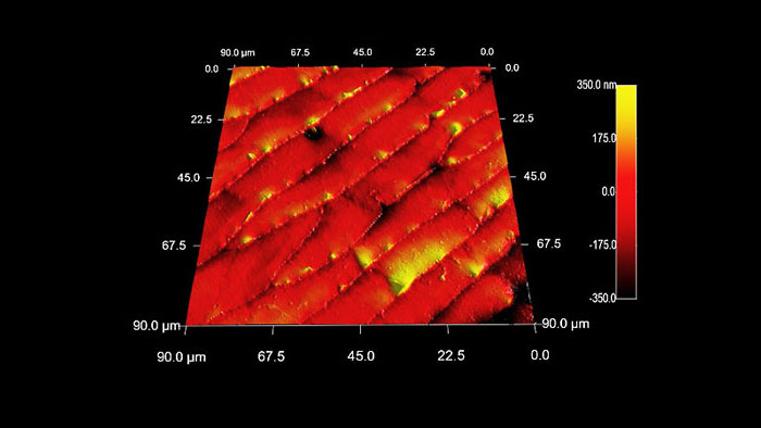
蟻の腹部の表面形状
Scanned with a BudgetSensors Tap300Al-G AFM プローブ 90 umスキャン
Image courtesy of Scott MacLaren, University of Illinois at Urbana-Champaign, USA
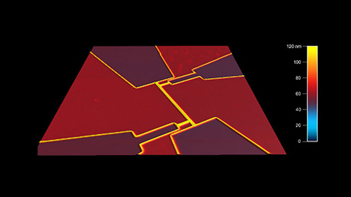
4オングストロームのステップを持つストロンチウムチタン酸化物(SrTiO3)表面
Scanned with a BudgetSensors Tap300Al-G AFM プローブ, 2umスキャン
Image courtesy of Scott MacLaren, University of Illinois at Urbana-Champaign, USA
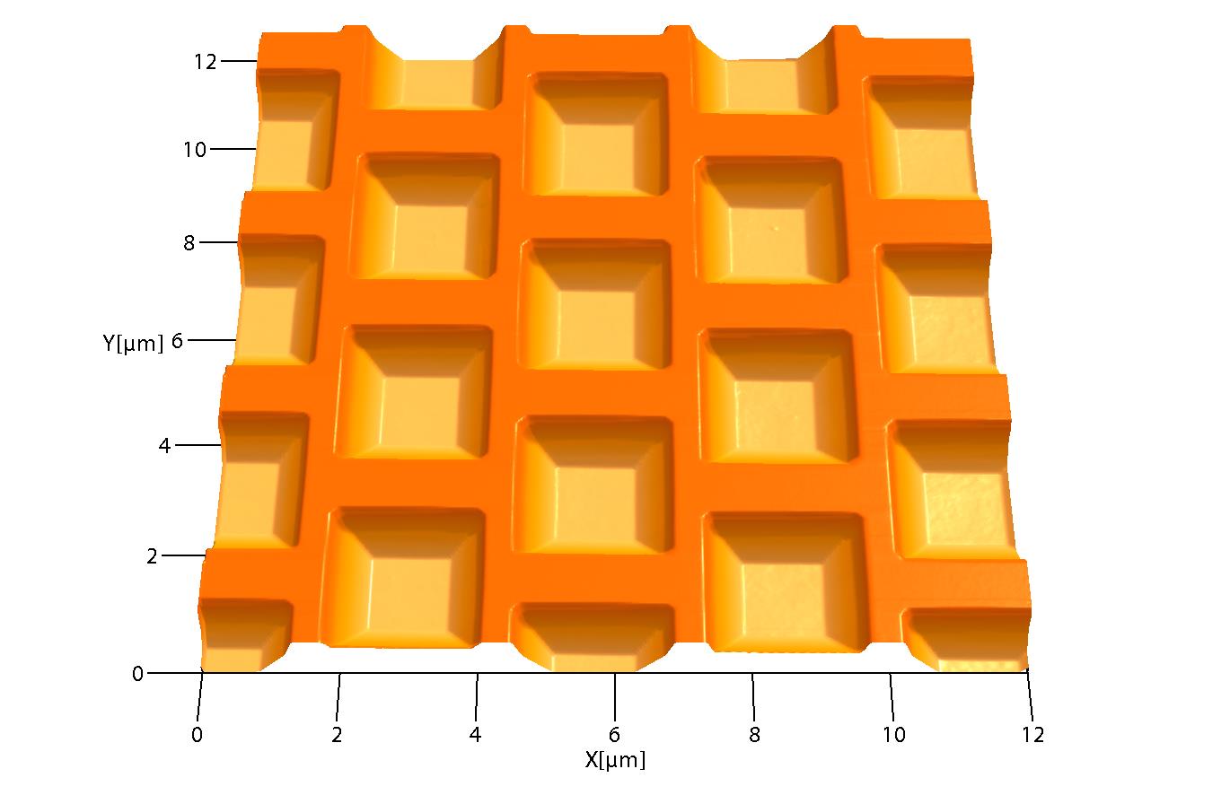
Mikromasch TGXキャリブレーショングレーティングの表面形状
Scanned with a OPUS by MikroMasch 240AC-NA AFMプローブ, 12 umスキャン
Image courtesy of Dr. Penka Terziyska, Innovative Solutions Bulgaria
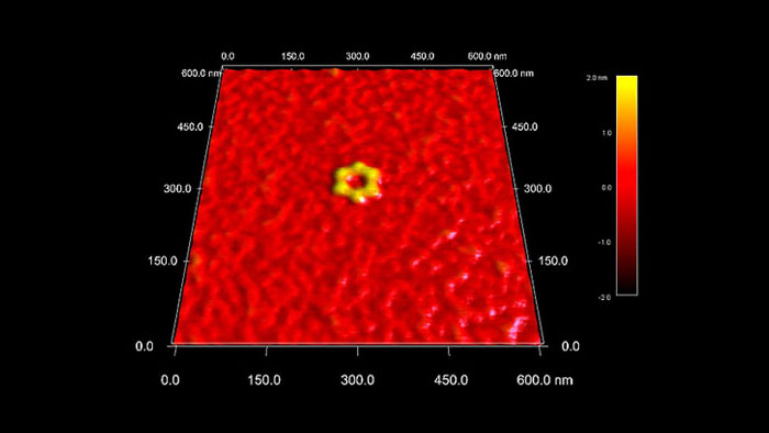
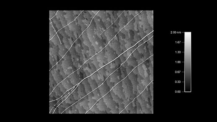
六角形を形成するDNA
Scanned with a BudgetSensors Tap300Al-G AFMプローブ, 600 nmスキャン
Image courtesy of Scott MacLaren, University of Illinois at Urbana-Champaign, USA
宇宙船のイオンスラスターの排気の溶融銅液滴が衝突したシリコン表面
Scanned with a BudgetSensors Tap300Al-G AFM probe, 25 micron scan
Image courtesy of Scott MacLaren, University of Illinois at Urbana-Champaign, USA
コンパクト ディスク (CD) の情報は、反射アルミ箔のすぐ下のプラスチック表面にある物理的な穴のバイナリ パターンによって保存される。 CD の録音 (または「書き込み」) 中に、これらの穴は、PC やラップトップの CD/DVD プレーヤーのレーザーによって文字通りプラスチックに焼き付けられる。
Scanned with a BudgetSensors Tap300-G AFMプローブ, 25umスキャン
Image courtesy of Dr. Yordan Stefanov ISB, Bulgaria
サファイア基板にフェムト秒レーザーパルスを照射し、その後アニールしてステップ構造を形成します。最表面は単一原子ステップ (3 Å) で覆われています。
Scanned with a BudgetSensors Tap300Al-G AFMプローブ, 20 umスキャン
Image courtesy of Scott MacLaren, University of Illinois at Urbana-Champaign, USA
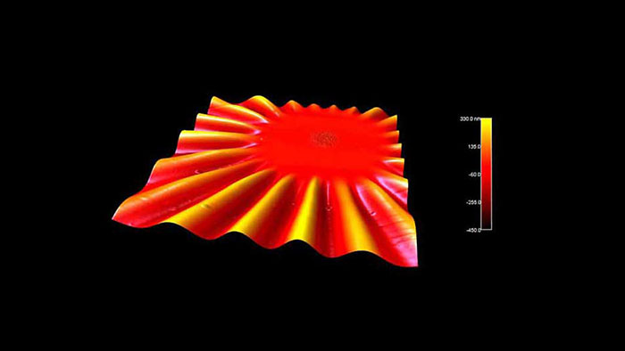
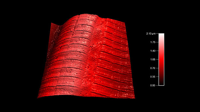
短いレーザーパルスで加熱した後の、ニッケルナノ粒子を含む非常に薄い (30 nm) 自立窒化ケイ素薄膜。ナノ粒子が基板と反応し、膜内に誘発された応力により膜表面に大きな波紋が生じている。
Scanned with a BudgetSensors Tap300Al-G AFM プローブ 90 umスキャン
Image courtesy of Scott MacLaren, University of Illinois at Urbana-Champaign, USA
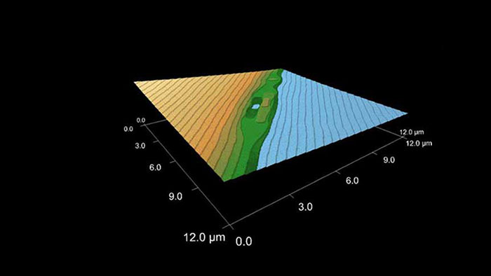
集束イオンビーム (FIB) で削られた酸化マグネシウム (MgO) 結晶。上部の加工されていない表面には、単一および二重の原子ステップが示されています。
Scanned with a BudgetSensors Tap300Al-G AFM プローブ, 20 umスキャン
Image courtesy of Scott MacLaren, University of Illinois at Urbana-Champaign, USA
ガラス上のポリ(ベンジル-ベータ-L-グルタミン酸)結晶
Scanned with a BudgetSensors Tap300Al-G AFMプローブ, 30 umスキャン
Image courtesy of Scott MacLaren, University of Illinois at Urbana-Champaign, USA
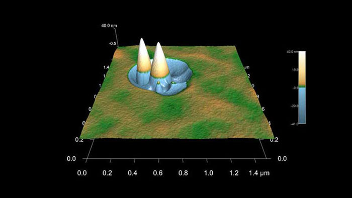
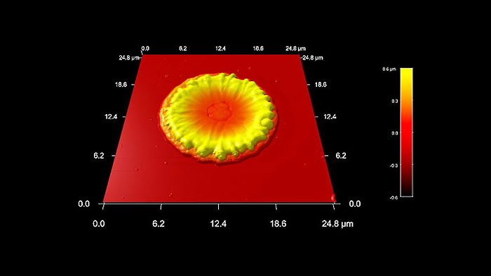
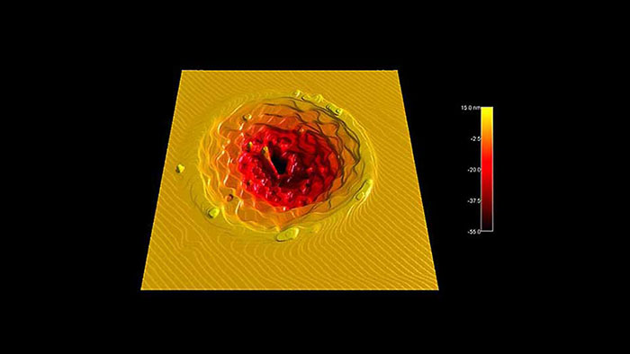
スパッタリング前の表面上の汚染物質が、典型的なスパッタ コーンの形成を引き起こす。
Scanned with a BudgetSensors Tap300Al-G AFM プローブ, 1.5 umスキャン
Image courtesy of Scott MacLaren, University of Illinois at Urbana-Champaign, USA
1400℃でアニールした後のサファイア結晶。原子ステップと時折欠陥のある清浄面を見ることができる。ステップの高さは約 3 Å 。
Scanned with a BudgetSensors Tap300Al-G AFM プローブ 12 umスキャン
Image courtesy of Scott MacLaren, University of Illinois at Urbana-Champaign, USA
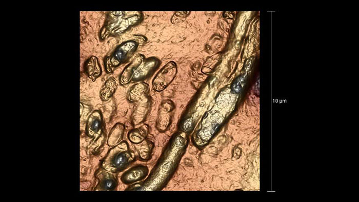
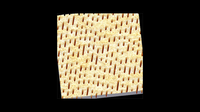
ジャガイモ寒天培地中のザントモナス カンペストリス菌
Scanned with a BudgetSensors Multi75-G AFM プローブ タッピングモード , 10umスキャン
Image courtesy of Dr. Yordan Stefanov, Innovative Solutions Bulgaria
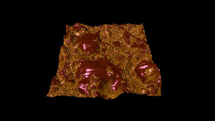
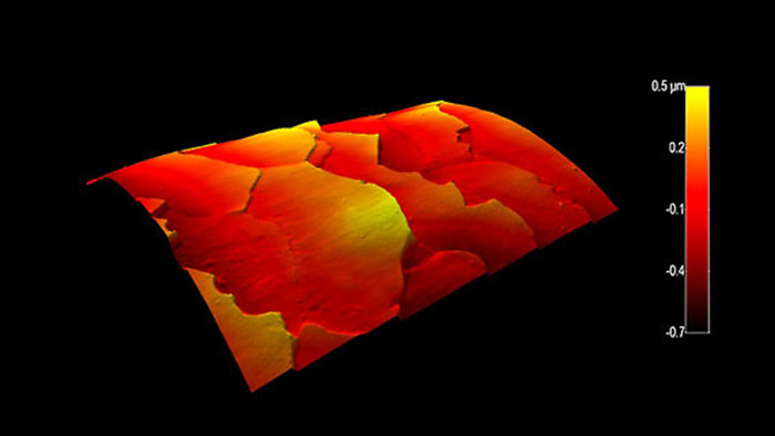
チョコレートは、主に細かく結晶化した連続した脂肪脂質マトリックス (ココアバター) からなり、その中にココアパウダーと砂糖粒子が分散した複雑な物質である。時間の経過とともに、脂質の結晶が結合してミクロンスケールの大きな結晶を形成する傾向があり、チョコレートの食感や味に大きな影響を与えている。この画像は、熟成させた市販のダーク チョコレート。表面形状を 3Dで表示し 、位相像をカラーデータとしてオーバーレイした。組成の違いを強調表示している (暗い部分は成長するココアバターの結晶)。
Scanned with a BudgetSensors Tap300Al-G AFM プローブ, 15 umスキャン
Image courtesy of Scott MacLaren, University of Illinois at Urbana-Champaign, USA